1 EEVblog #939 - How Is A PCB Manufactured?
Dave Jones' walk through a professional PCB factory, used to show how boards are etched, masked and silkscreened in practice.
Topic
8 videos. Ranked by independent recommendations, not by views.
Dave Jones' walk through a professional PCB factory, used to show how boards are etched, masked and silkscreened in practice.
EEVblog's look at SMD thermal jumpers is recommended for moving heat around a board, with a further remark on how solder mask affects cooling.
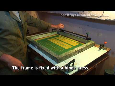
Linked as an illustration of screen-printing circuit boards in a small workshop, including how solder mask goes on, with one person asking whether board houses work this way.
Cited for its technique of removing solder mask on a CNC using a spring-loaded drag bit that stops at the copper, avoiding some bed-levelling trouble.
Recommended for learning how clean a surface truly is, why solvents differ, and how to check a part before applying epoxy or solder mask.
A tour of a commercial PCB plant, recommended for seeing how layers, etching and solder mask are actually produced and how far that sits from home methods.
Robert Feranec's EasyEDA tutorial is recommended as a route into PCB design, including finishing details such as making a gold logo through the solder mask.
Cited as an example of repairing a board by exposing bare copper under the mask and bonding a component or wire to the trace.